
9. Command and Data Handling
9.5 Typical Avionics

In spacecraft history, computers have come a long way from core rope memory on the Apollo Guidance computer to millions of transistors on a chip smaller than your fingernail. This section will give an overview of the different modern hardware components in an onboard computer.


The on-board processor, or flight computer, holds the clock, Central Processing Unit (CPU), Graphics Processing Unit (GPU), maybe a Field-Programmable Gate Array (FPGA), memory storage, and other circuitry so that these components can communicate with each other. If you are super ambitious, you may pick your own components and create your own onboard computer, which is an immense feat. More likely, you will survey available options and weigh the tradeoffs of the components of this one flight computer to another flight computer. This chapter will discuss the core components of a flight computer that you should pay attention to when selecting avionics.


Clocks
Crystal Oscillator


“A crystal oscillator is an electronic oscillator circuit that uses the mechanical resonance of a vibrating crystal of piezoelectric material to create an electrical signal with a constant frequency” [Wikipedia]. The most common piezoelectric resonator is the quartz crystal and when incorporated into an oscillator circuit is called a crystal oscillator. The quartz crystal may be manipulated to oscillate at a precise frequency by applying voltage on and off. These oscillators operate from a few tens of kilohertz to hundreds of megahertz. Quartz crystals are found in the majority of timekeeping technology, like wristwatches, computers, and wall clocks.
The stability of the crystal’s frequency depends on the crystal’s Q factor or the degree of underdamped response. We want a high Q factor where the vibration is not damped much or in other words, energy is not lost. Environmental changes of temperature, humidity, pressure, and vibration can change the resonant frequency of a quartz crystal. Spurious frequencies (undesired frequencies) can occur if the crystal is subject to vibration (something to test for after conducting an environmental vibration test on a shake table!). During manufacturing and assembly, the crystal may experience mechanical stress due to bonding and mounting or thermal expansion throughout the crystal’s operational lifetime. Permanent changes can occur if the crystal incurs mechanical damage due to shock, which can tear crystals off their mountains or crack the crystal. Due to the space environment, the composition of the crystal may permanently change due to the crystal itself outgassing or surrounding hardware outgassing onto the crystal. Space radiation can affect the Q factor of the clock, altering the natural frequency of the oscillator. “Crystals have no inherent failure mechanisms; some have operated in devices for decades. Failures may be, however, introduced by faults in bonding, leaky enclosures, corrosion, frequency shift by aging, breaking the crystal by too high mechanical shock, or radiation-induced damage when non swept quartz is used. Crystals can be also damaged by overdriving” [Wikipedia].


The important result of clock degradation is clock drift. “By space navigation standards, quartz crystal clocks aren’t very stable. After only an hour, even the best-performing quartz oscillators can be off by a nanosecond (one billionth of a second). After six weeks, they may be off by a full millisecond (one-thousandth of a second), or a distance error of 185 miles (300 kilometers). That would have a huge impact on measuring the position of a fast-moving spacecraft” [NASA]. When the spacecraft is not in communication with the ground, the flight computer relies on the onboard clock as the sole clock. A crystal oscillator may be unstable and oscillate at an imprecise frequency, which leads to clock drift. The spacecraft’s clock, based on the crystal oscillator, may diverge from the mission operator’s reference clock, potentially affecting time-sensitive operations. Corrections can be made to the spacecraft’s clock when mission operators contact the spacecraft or when the spacecraft communicates with other spacecraft with more precise clocks; GPS atomic clocks are a good reference but even these satellites must be corrected twice a day from ground-based clocks.
Artemis Kit Specific
The Artemis CubeSat Kit has MIMXRT1062 from the Teensy 4.1 and a BCM2835 single-core processor on the Raspberry Pi Zero W.
Atomic Clock

Atomic clocks also use frequencies of natural phenomena, but instead of mechanical vibration, atomic clocks measure the electromagnetic signal of electrons as a radioactive element decays. Atomic clocks are considered the “most accurate time and frequency standards known” [Wikipedia]. In fact, the way we keep time on Earth is by averaging measurements of various atomic clocks around the world, called the International Atomic Time (TAI), an international effort in which NIST and NASA JPL are involved. This method is so precise that scientists have defined the “SI unit of a second in terms of exactly 9 192 631 770 oscillations of the cesium atom” [Wikipedia].

The most famous implementation of an atomic clock in space is GPS satellites. Because GPS receivers must measure time delays of signals, having a precise clock is of utmost importance. “GPS Time (GPST) is a continuous time scale and theoretically accurate to about 14 ns” [Allan]. Other satellites that rely on atomic clocks are the Global Navigation Satellite System, the Galileo Global Navigation Satellite System, and the Deep Space Atomic Clock. Atomic clocks used to be reserved for missions that specifically need nanosecond precision timekeeping as the cost and development could be prohibitive. A single microsecond of inaccuracy on a GPS satellite relates to 300 m of error. A commercial atomic clock used to cost on the order of 30,000 USD but with technological advances, you could have your very own miniature atomic clock for 1,500 USD [PhysicsWorld]!

NIST Launches a New U.S. Time Standard: NIST-F2 Atomic Clock video courtesy of YouTube
A variant of the atomic clock is the quantum clock that utilizes “laser-cooled single ions confined together in an electromagnetic ion trap. Developed in 2010 by physicists as the U.S. National Institute of Standards and Technology, the clock was 37 times more precise than the then-existing international standard. NIST has attributed the clock’s accuracy to the fact that it is insensitive to background magnetic and electric fields, and unaffected by temperature.” [Wikipedia]. These clocks have not been demonstrated in space but are fun to think about for potential technology demonstrations of the state of the art.
Watchdog Timer
“A watchdog timer (sometimes called a computer operating properly or COP timer, or simply a watchdog) is an electronic or software timer that is used to detect and recover from computer malfunctions. During normal operation, the computer regularly resets the watchdog timer to prevent it from elapsing, or “timing out”. If due to a hardware fault or program error, the computer fails to reset the watchdog, the timer will elapse and generate a timeout signal. The timeout signal is used to initiate corrective actions. The corrective actions typically include placing the computer system in a safe state and restoring normal system operation. Watchdog timers are commonly found in embedded systems and other computer-controlled equipment where humans cannot easily access the equipment or would be unable to react to faults in a timely manner. In such systems, the computer cannot depend on a human to invoke a reboot if it hangs; it must be self-reliant. For example, remote embedded systems such as space probes are not physically accessible to human operators; these could become permanently disabled if they were unable to autonomously recover from faults. A watchdog timer is usually employed in cases like these” [Wikipedia]. The watchdog timer is critical for fault detection as its only function is to serve as a reboot if something goes wrong. The watchdog is typically connected directly to the CPU and fed the same clock measurements.

Processors
CPU

The CPU is the main computing unit of the brain, managing high-level processes in series like how our cerebrum manages reading, thinking, learning, speech, emotions, and planned muscle movements. The CPU is made of millions of individual transistors, “contained on a single metal-oxide-semiconductor (MOS) integrated circuit (IC) chip” [Wikipedia]. Transistors form the basis of integrated circuits, turning signals on or off, which is the basis of binary data. “There are 2 parts of the CPU: The ALU and Control Unit. The Arithmetic Logic Unit (ALU) performs arithmetic operations (such as addition and subtraction) and logical operations (such as comparing two values). The Control Unit deciphers and carries out instructions. Different CPUs have different types of instructions, so software made for one type of CPU will not run on other kinds” [Gusta]. CPUs are typically classified by the number of cores onboard, where each core is a computing unit that could focus on one task. Today, a multi-core (more than one core) processor can handle multiple tasks simultaneously. When selecting a CPU, pay attention to:
-
- Instructions per second – For spacecraft missions, instructions per second relate to the required throughput and processing necessary to run executions in a software environment. Clock speed is not everything (see Megahertz Myth).
- FLOPS – The number of floating-point operations per second is often important in selecting computers for scientific computations.
- Performance per watt – For a power-constrained system, this particular metric is very important for spacecraft evaluating relative or scaleable power consumption.
- Low power – For systems with limited power sources like spacecraft, this metric evaluates absolute maximum power consumption.
- System designers building real-time computing systems want to guarantee a worst-case response. This metric relates to handling faults during the spaceflight mission.
Small size or low weight – Compact volume or low mass options are encouraged for spacecraft systems.

The common manufacturers for CPUs on the ground are Intel, AMD, and ARM. The fundamental distinction between these companies is their instruction set architectures. Intel holds the patents to x86, AMD to x64, and ARM has created its own ARM architecture. The general differences between the three companies are summarized by Nachman Networks:
“Intel is the most popular and well-known maker of processors. Manufacturers like Dell, Apple, Samsung, and HP all use Intel processors in their computers. Intel processors are the most stable and offer the best all-around performance. The current i3, i5, and i7 models represent entry, middle and high-level hardware.
-
- AMD is Intel’s biggest competitor, offering processors that are similar to Intel’s, but at a, for the most part, cheaper price. The majority of computer manufacturers, except for Apple, also offer products with AMD processors. AMD’s Athlon processors are budget models while Phenom and FX are mainstream and high level respectively.
- ARM processors are generally used in smartphones, mobile devices, and tablets. Apple’s iPhone and iPad; Samsung’s Galaxy line and HTC devices all use some form of ARM processor in their mobile devices. A rule of thumb is, if it doesn’t have AMD or Intel in the name, it’s most likely an ARM processor”.
In space, processing power lags far behind progress on the ground due to the need for radiation hardening and space radiation testing. “The Intel 386SX that ran the so-called “glass cockpit” in space shuttles was clocked roughly at 20MHz. As we near 2020, the RAD750 stands as the state-of-the-art, single-core space-grade processor. Curiosity uses two BAE RAD750 processors clocked at up to 200MHz” [Krywko]. The RAD750 is based on the PowerPC 750, created by IBM and Motorola in 1997 to compete with Intel. The RAD750 costs $200k. “The BAE RAD5545 is probably the most powerful radiation-hardened processor available today”, clocking at 466MHz [Krywko]. ESA has developed the LEON line of space-grade processors working in SPARC architecture, which is open source. The latest LEON processor is the quad-core GR740 clocked at roughly 250MHz. In the future, we can expect the development of the High-Performance Spaceflight Computing (HPSC), based on the ARM Cortex A53 quad-core processor and expected to clock between 1.2 to 1.8 GHz.

A few types of integrated processors include microcontrollers, digital signal processors, and microprocessors. Microprocessors (PP) are processors on an integrated circuit that are “multipurpose, clock-driven, register-based, digital integrated circuits that accept binary data as input, process it according to instructions stored in its memory, and provide results (also in binary form) as output” [Wikipedia]. Microprocessors are the most powerful of the CPU integrated circuits and also consume the most power, ranging from 50W – 200W. They provide > 1GIPS, 4GB+ RAM, ROM storage, HD’s, CD-ROM’s, etc. Microprocessors use a general-purpose instruction set. When you think of the most advanced commercial processors, like Intel’s latest Core i9 processors, these are microprocessors. Microprocessors live on your laptop, your cellphone, your desktop. They are the more general-purpose, workhorse computing unit. Microprocessors have been used increasingly in spacecraft and are most likely the central computing unit of modern spacecraft [Wikichip].

Microcontrollers are small, dedicated processors to perform very specific tasks with clock speeds of about 1-100MHz, <16MB RAM, Read-Only Memory storage (no HD/Mass storage). Microcontrollers are everywhere, in “computer keyboards, monitors, printers, copiers, fax machines, microwave ovens, washers and dryers, security systems, lawn sprinkler station controllers, and music/video entertainment components” [Farahman]. These products have specific, repetitive tasks and do not have intelligence or adaptability. Specific subsystem components may come with their own microcontrollers to offer low-level control with which the central onboard computer must communicate with. These subsystems and applications may include [ESA]:
-
- propulsion system control
- sensor bus control
- robotics applications
- simple motors control
- mechanisms control
- power control
- radiation environment monitors
- thermal control
- antenna pointing control
- In-situ ionospheric plasma measurements [Haas et al.]
- Altimeter data [Perschy et al.]
- Terrestrial communications [Lefevre et al.]
- ACS/GNC sensors (Gyroscope, IMU, Magnetometer)

Digital signal processors (DSP) are specialized microprocessor chips, specifically designed to manage embedded digital systems and digital signal processing. “They are widely used in audio signal processing, telecommunications, digital image processing, radar, sonar, and speech recognition systems, and in common consumer electronic devices such as mobile phones, disk drives, and high-definition television (HDTV) products”, with the goal to typically measure, filter, or compress continuous real-world analog signals [Wikipedia]. DSPs have a high processing/power ratio (e.g., 1GMIPS @ <6W) with clock speeds typical of 100MHz – 1GHz, 16MB to 2GB RAM, Read-Only Memory storage, and FLASH storage. DSPs will most likely be tied with the spacecraft payload for data-intensive missions to process experiment data or with telecommunication subsystems:
-
- In-situ ionospheric plasma measurements [Haas et al.]
- Altimeter data [Perschy et al.]
- Terrestrial communications [Lefevre et al.]
Suggested Readings
Space Technology 8 – Dependable Multiprocessor https://www.jpl.nasa.gov/nmp/st8/tech/eaftc_tech1.php
GPU

GPUs are power-efficient, computational workhorses that specialize in processing image data, like our visual cortex. “Energy efficiency is one of the most important factors that will affect a broader adoption of GPUs in high-performance computing” [Jiao]. GPUs have smaller cores than CPUs, which means each core cannot accept the same relative quantity of instructions. GPUs tend to have much longer pipelines, which is advantageous if a computational task can be broken down into several similar subtasks, processed, and then combined upon completion. “While it does not decrease the processing time for a single data instruction, it increases the throughput of the system when processing that data” [Wyrwas].
GPUs have seen wide adoption on the ground during the rise of machine learning and data analytics, utilized for heavy data processing [NVIDIA]. “The first satellite to include a GPU for image compression was COROT. COROT is a French national space agency (CNES)-that led a mission to detect exoplanets orbiting other stars and to probe the mysteries of stellar interiors. GPUs and other SoC/SiP devices are highly susceptible to radiation effects. Many types of radiation may affect GPGPU logic in operation due to Single Event Transients (SET)15, corrupting the logic outcome and producing an erroneous result, and eventually being placed into the memory, thus very similar to a Single Event Upset (SEU). The radiation fault could be masked or even propagate to the output generating single or multiple silent data corruptions. The difference between both events is the former affects logic circuits and the latter memory elements. In either situation, the device can have functional interruptions or even hang” [Wyrwas]. Despite the risks, the potential benefit of high-performance computation can be had with rigorous testing and/or radiation protection (refer to the suggested reading or read on to the Testing and Verification section in this chapter).
GPU devices depend on the application environment or purpose. They include:
-
- Native GPU (i.e. Nvidia GeForce)
- Application Processor (i.e. TI OMAP)
- Accelerator Processing Unit (i.e. AMD’s Fusion APU)
- ASIC/FPGA/PLD (i.e. Xilinx Zynq UltraScale+ MPSoC)
Potential project vendors include Intel, Nvidia, Apple, Arm, Qualcomm, Marvell, Vivante, MediaTek, AMD, Texas Instruments, Altera, Xilinx, PowerVR, STMicroelectronics-Ericsson, IBM, and ZiiLABS.
Suggested Reading
Body of Knowledge for Graphics Processing Units (GPUs)
https://nepp.nasa.gov/files/29564/NEPP-BOK-2018-Wyrwas-GPU-TN60884.pdf
FPGA

FPGAs are reconfigurable integrated circuits that encode processes directly into the hardware without input from the CPU, like a spacecraft’s muscle memory. “One of the benefits of FPGAs over processor-based systems is that the application logic is implemented in hardware circuits rather than executing on top of an OS, drivers, and application software. Modern FPGAs contain components that are specialized for specific functions as well as more general-purpose configurable logic. The combination of dedicated functionality components with the configurable logic has allowed for architectures that consume less power and perform more efficiently” [Eastland]. FPGAs can be configured into a specific hardware configuration after fabrication by loading compiled software “containing information on how the components should be wired together”, called Hardware Descriptor Language [NI]; you can liken this ability to shapeshifting. This configuration can even happen remotely while the FPGA is in space! FPGAs are generally fast, reliable, and flexible but are susceptible to the effects of space radiation.

“FPGAs are sensitive to both heavy ion and proton-induced single event upsets (SEUs). Single-event upsets in the FPGA affect the user design flip-flops, the FPGA configuration bitstream, and any hidden FPGA registers, latches, or internal state” [Wirthlin]. To mitigate these radiation effects, we can resort to hardware redundancy or triple modular redundancy, which is implementing multiple circuits with the same functionality voting on a process result. Another mitigation technique could be to “scrub” the FPGA configuration and reconfigure the FPGA periodically.
“Historically, there have been two basic options for FPGAs in space applications: high-density, re-programmable, conventional SRAM-type FPGAs – repurposed and heavily modified for space use; and lower-density, non-volatile, one-time-programmable, anti-fuse devices designed specifically for space applications. The former were usually supplied by Xilinx and fit primarily into “payload” type applications. The latter were usually supplied by Microsemi (formerly Actel) and were suitable for mission-critical flight control and similar applications” [Morris]. Specifically, “there are three FPGAs that comprise the majority of current space-qualified FPGA needs: the Xilinx Virtex-5QV (SRAM, 65nm), the Microsemi RTG4 (Flash, 65 nm), and the Microsemi RTAX (Anti-fuse, 150 nm)” [Lee]. Most modern commercial FPGA systems tested so far perform well in radiation and there is a potential path to flight, but as of right now, these circuits are not readily adopted as they are considered risky.

Memory
Memory stores information for immediate use in a computer. This section will define different memory types, their functions, and use cases. A defining characteristic of memory is its volatility. Volatile memory is stored temporarily and is lost when the divide is powered off. Non-volatile memory is stored permanently and the data remains stored even if it is powered off [geeksforgeeks.org]. Volatile memory has decreased capacity, and increased power dissipation, but comes with fast access times and throughput. Applications include run-time memory and buffering. Non-volatile memory has greater capacity, and lower power dissipation but comes with slower access time and throughput. Applications include start-up memory and persistent storage [Troxel].
Read-Only Memory (ROM)
Read-only memory is as the name suggests: read-only. This type of non-volatile memory is defined by the manufacturer and cannot be changed. ROM is typically advantageous for storing software that does not change through the system lifetime, usually dedicated to the firmware. Although ROM can be re-programmed with special instructions and unusual voltage settings, ROM can only be rewritten a limited number of times. A famous use case of ROM is the CD-ROM, clear in the naming convention. A widely used case of ROM today includes USB flash drives.

Historically, the core rope was used in NASA/MIT’s Apollo Spacecraft Computers, DEC’s PDP-8 computers. The core rope is a form of transformer matrix ROM, “programmed by handweaving ‘world line wires’ inside or outside of ferrite transformer cores” [Lumen]. Today, electrically erasable programmable read-only memory (EEPROM) is typically used to store a small amount of data for a startup, like a device configuration, calibration tables, boot code, and debug information [Troxel]. The structure of an EEPROM consists of arrays of floating gate transistors, providing data persistence and relatively strong Total Ionizing Dose and Single Event Effect performance. EEPROM includes control circuitry that is susceptible to radiation. Typical device capabilities include:
-
- 32Kb to 256Kb options
- ~1,000,000 rewrite cycles
- ~10-year data retention or more
- 10K to 1M rad TID tolerance
Commercial options include Actel, Aeroflex, Atmel, Hitachi, Infineon, Maxwell, Samsung, etc. EEPROM technology is used for credit cards, SIM cards, and keyless entry.

Random Access Memory (RAM)
Random-access memory (RAM) is computer memory that can be read and changed typically used to store working data and machine code [Wikipedia]. RAM is volatile memory, which is lost when power is removed and/or after a reset. RAM is a fast memory available, running at over 1000 MHz. There are two types of RAM: static RAM (SRAM) and dynamic RAM (DRAM).

SRAM is typically used for control processing applications, like buffering between cache and storage and as the processor’s “main memory”. SRAM cells use latching circuitry (flip-flop) to store each bit. “Self-reinforcing nature improves SEE performance and SEFI modes not as varied and often not as complex” [Troxel]. Commercial options include Aeroflex, BAE, Honeywell, Maxwell, Samsung, etc. Typical device capabilities include:
-
- 4Mb to 64Mb options typical
- “infinite” rewrite cycles
- No data retention
- 100K to 1M rad TID tolerance typical
~10ns access latency typical

DRAM is typically used for data processing applications, much like SRAM but for data. Instead of latching circuitry, DRAM consists of tiny capacitors and transistors to store memory. Capacitors leak in charge so “DRAM requires an external memory refresh circuit which periodically rewrites the data in the capacitors, restoring them to their original charge. This refresh process is the defining characteristic of dynamic random-access memory, in contrast to static random-access memory (SRAM) which does not require data to be refreshed” [Wikipedia]. Complex addressing and refresh modes increase Single Event Functional Interrupts. DRAM is extremely common in personal computers. Flash memory eventually fails given a high enough Total Ionizing Dose, up to 200 Krads from a 2011 study [Oldham]. TID performance is continually improving, due to smaller feature size reduction “tricks”. Typical device capabilities include [Troxel]:
-
- 2Gb to 8Gb options typical
- “infinite” rewrite cycles
- No data retention
- Variable TID tolerance
- ~50ns access latency typical
Commercial options include Hyundai, Micron, Samsung, etc.
Flash Memory or Non-Volatile Random Access Memory (NVRAM)

The best-known form of NVRAM and EEPROM is flash memory. Flash memory is a type of non-volatile memory, based upon Electrically Programmable Read-Only Memory (EPROM) technology. Flash is between ROM & RAM mid-speed memory, which can be easily read and written. Flash memory is typically used to store large amounts of data for a startup, like a device configuration, calibration tables, boot code, and debug configuration. Flash usually stores “software/firmware” that is expected to be updated but otherwise does not change during normal operations. Flash has been very common in recent space applications. “Radiation removes (or masks) electrons from the floating gate which causes bits to be in error”, as seen in the figure below[Kay et al.]. Typical device capabilities include [Troxel]:
-
- 256Mb to 8Gb options typical
- ~5,000 to ~500,000 rewrite cycles
- ~20-year data retention or more
- 5K to hundreds of K rad TID tolerance typical (ELDRS effects)
Commercial options include Hynix, Intel, Micron, Samsung, Spansion, etc. Xilinx offers flash-based configuration memory as well.

Artemis CubeSat Kit RAM
Mass Storage
Hard Disks/Drives
Hard disk drive (hard drive, hard disk, or fixed disk) is an electromagnetic data storage device that relies on magnetic storage to retrieve digital data. Hard disk drives (HDDs) are a type of non-volatile storage that can store up to terabytes of data. These hard drives are tremendously common within personal computers and also as external storage devices. These mass storage devices are susceptible to the vibrations of a harsh launch environment. The angular momentum of the disk in the hard drive could affect the angular momentum of the spacecraft. The rotation rate of the disk also makes the hard drive susceptible to mechanical failure, which would be critical to the mission. Due to these reasons, HDDs are not preferred for spacecraft missions.

Solid-State Drives

Solid-state drives (SSDs) do not use mechanical parts, like the hard drive, but use only electronic circuits to read and write digital information. Solid-state storage is a type of non-volatile memory that typically utilizes electrically programmable non-volatile flash memory. Radiation affects SSDs in the same way that radiation affects flash memory. SSDs are faster than HDDs because of the lack of mechanical parts but are much more expensive. Still, they are the preferred storage device for space missions, like the Mars Reconnaissance Orbiter. Types of flash-based solid-state storage devices include the following [Wikipedia]:
-
- MultiMediaCard (MMC) – a memory card type used in portable devices
- Secure Digital (SD) – a memory card type available in different variants, speeds, and sizes, used extensively in portable devices
- Solid-state drive (SSD) – a computer storage device available in various form factors, with different interfaces, and in various classes targeting different market segments. The following components are susceptible to radiation effects and should be considered for radiation tolerance [Lamorie and Ricci]:
- The core NAND flash components
- The Flash Translation Layer controller
- Configuration memory used for the Flash Translation Layer controller
USB flash drive – pocketable removable storage devices that interface through USB, available in various shapes and sizes
Artemis CubeSat Kit Mass Storage
The Artemis CubeSat Kit uses a solid-state storage device, specifically the SD card.
Input/Output Interfaces
Input/Output (I/O) interfaces to exchange information between avionics components, like storage, sensors, processors, and memory. These interfaces include data buses, digital I/Os, analog/digital converters, and port connectors.
Data Bus

A spacecraft’s data bus connects all subsystems that generate and receive data/commands, similar to a power bus’s management of power to all subsystems. The data bus handles all the internal communications and passes data to the communications system for external communication. The data bus is in charge of quick, in-succession data routing and prioritization, as a switchboard operator. Data buses are reserved for high-speed data transfers (>33Mhz or >500Mbps), typically connecting the processor to peripheral subsystems to communicate 16, 32, or 64 bit wide messages. There are standards for data buses so that design teams don’t have to reinvent the wheel every time the avionics must be designed. These standards have a communication protocol, physical interface, data rates, and primary applications. The most prevalent standard for spacecraft is the MIL-STD-1553 and for CubeSat, the CubeSat Space Protocol.
The MIL-STD-1553 is a standard for an avionics data bus used in aerospace and military applications. There is 1 bus controller that initiates all exchanges and up to 30 remote terminals. The overall data bus architecture could include redundant MIL-STD-1553B buses, a bus controller, a backup bus controller, a bus monitor, a remote terminal, a subsystem embedded with a remote terminal, and a subsystem communicating with a remote terminal. The bus controller operates according to a command list stored in its local memory, commands the various remote terminals to send or receive messages, services any requests that it receives from the remote terminals, detects and recovers from errors, and keeps a history of errors. The bus monitor’s primary role is to monitor and record bus transactions. The remote terminal provides an interface between the MIL-STD-1553B data bus and an attached subsystem, and a bridge between a MIL-STD-1553B bus and another MIL-STD-1553B bus. The hardware includes cabling, stubbing, bus couplers, cable termination, and connectors. The bus operates at 1 MHz and between 18 – 27 V.


“A Controller Area Network (CAN bus) is a robust vehicle bus standard designed to allow microcontrollers and devices to communicate with each other’s applications without a host computer. It is a message-based protocol, designed originally for multiplex electrical wiring within automobiles to save on copper, but can also be used in many other contexts. For each device, the data in a frame is transmitted sequentially but in such a way that if more than one device transmits at the same time the highest priority device is able to continue while the others back off. Frames are received by all devices, including by the transmitting device” [Wikipedia]. “The controller area network (CAN) protocol is a proven, highly reliable communication system for harsh environments and has been used in automotive and industrial applications for over 30 years. Below is a list of the major features and benefits of the CAN protocol” [Renesas]:
-
- The simple two-wire bus topology reduces wiring and saves space and cost by eliminating bulky wiring harnesses.
- The ISO 11898 standards for the CAN controller and CAN transceiver ensures ECUs built by different manufacturers will work together when put into a CAN network.
- An ECU device can communicate with multiple devices at the same time.
- High transceiver driver output current drives double-terminated cables and long cables. Drives up to 120 devices at data rates up to 1Mbps.
- The CAN system of arbitration allows easy connection of multiple devices to the bus without any additional collision detection. Arbitration occurs automatically, without loss of data, and without increasing bus latency.
- Wide CMR of at least -2V to +7V. CAN allows networks to drive long cables in harsh environments where nodes may have large ground differences.
Error detection is built into the protocol for reliable communications

“The following outlines the advantages of employing a CAN bus communications network for data handling in space systems vs. the conventional MIL-STD-1553 and RS-485 point-to-point interface solutions. The figure above shows the comparison between the present conventional topology vs. the CAN two-wire broadcast topology. Several nodes can be added to a single bus. This significantly reduces system/cable costs while providing a cost-effective way to add functionality. According to ESA, a satellite’s weight and mass can be reduced by 10% to 18%. Weight/mass is proportionate to overall satellite and launch costs”:
-
- The CAN multi-master/multi-drop topology significantly reduces the amount of wiring and connectors.
- Replaces older, more costly communication protocols.
- CAN has lower power consumption vs. the conventional MIL-STD-1553 systems.
- Data prioritization and data contention are advantages over other protocols.
- Adds several million dollars of functionality.
CAN enables scalable bus architectures with increased reliability, observability, and controllability.

For smaller spacecraft, the CubeSat Kit Bus (CSKB) is a stackable connector with 104 pins. The CSKB “utilizes the same physical connectors as the industry-proven PC/104 bus” [Pumpkin]. Of the 104 total pins, the CSKB offers 28 Input/Output (I/O) pins to interface with the subsystems. “Additional pins from the PPM processor to the CubeSat Kit Bus connector include power and ground, Deployment Switch and Remove-Before-Flight Switch direct bussed connections, transceiver data and control signals, user signals, analog references, and miscellaneous control signals” [Pumpkin].

The PC/104 standard allows modular stacking of boards that can expand functionality. A common PC/104 system will stack a CPU board, power supply board, and peripheral boards. For spacecraft, these boards could include a payload board, telecommunications board, ADCS board, etc. Most PC104 boards include standard PC interfaces like Serial Ports, USB, Ethernet, and VGA. These Input/Output interfaces will be expanded upon in a later section of this chapter. The PC/104, coupled with an x86 instruction set architecture, can run standard PC operating systems, like DOS, Linux, or Windows.
Artemis Kit Specific
Artemis CubeSat Data Bus
- The Artemis CubeSat Kit uses the PC/104 or CubeSat Kit Bus architecture.
Digital and Analog I/O
“The main purpose of I/O interfaces is to transmit and receive data” [Smith]. To format the raw subsystem input data in a digestible way for the processor or whatever end node, the data must pass through an interface that modifies the data format. These interfaces could manipulate digital or analog signals and can be unidirectional or bidirectional. These interfaces can consist of port connectors, circuitry, and wire harnessing.

The most basic interface is an analog-to-digital converter, or ADC, which converts analog signals to digital signals. The conversion involves quantization of the input, so it necessarily introduces a small amount of error or noise. Additionally, the data product’s bit size affects that accumulation of error; fewer bits, more error.

“A digital I/O board is an interface board that adds the ability to input and output digital signals in parallel to a computer” [Contec]. There are various and many applications for digital I/O interfaces that can be connected in series. A common series connection could be a sensor outputting an analog signal, connected to an analog-to-digital converter, then a digital I/O interface, then the data bus, then finally to the processor.
Port Connectors

Port connectors allow electrical signals to pass through physical connections, think of the end of a USB cable that goes into your computer. There are many different types of connector types that have their own communication standards. Different port connectors are historically used for specific applications and carry unique advantages/disadvantages. “The benefits of using commercially based networking standards and protocols have been widely discussed and are expected to include reduction in overall mission cost, shortened integration and test (I&T) schedules, increased operations flexibility, and hardware and software upgradeability/scalability with developments ongoing in the commercial world” [Webb and Day]. Characteristics include baud rate, communication protocol, differential configuration, directionality, synchronicity, etc. “Baud rate is a measure of the speed of data transfer, expressed in bits per second (bps). The bits of data can be transmitted either in parallel or serial form. In parallel communication, the bits of data are sent all at the same time, each through a separate wire. In serial communication, the bits are sent one by one through a single wire” [CircuitBasics]. This section will give an overview of these various port connections.

“The general-purpose input/output (GPIO) is an uncommitted digital signal pin on an integrated circuit or electronic circuit board which may be used as an input or output, or both, and is controllable by the user at runtime. GPIOs have no predefined purpose and are unused by default. If used, the purpose and behavior of a GPIO are defined and implemented by the designer of higher assembly-level circuitry: the circuit board designer in the case of integrated circuit GPIOs, or system integrator in the case of board-level GPIOs. Many circuit boards expose board-level GPIOs to external circuitry through integrated electrical connectors. Usually, each such GPIO is accessible via a dedicated connector pin. GPIOs are also found on embedded controller boards such as Arduino, BeagleBone, Teensey, and Raspberry Pi” [Wikipedia]. The Artemis CubeSat Kit has a Teensy.

A universal asynchronous receiver-transmitter (UART) is used for asynchronous serial communication in which the data format and transmission speeds are configurable. “The hardware for UART can be a circuit integrated on the microcontroller or a dedicated integrated circuit. Today, UART is being used in many applications like GPS Receivers, Bluetooth Modules, GSM and GPRS Modems, Wireless Communication Systems, RFID based applications, etc” [ElectronicsHub].


“UARTs transmit data asynchronously, which means there is no clock signal to synchronize the output of bits from the transmitting UART to the sampling of bits by the receiving UART. Instead of a clock signal, the transmitting UART adds start and stop bits to the data packet being transferred. These bits define the beginning and end of the data packet so the receiving UART knows when to start reading the bits. When the receiving UART detects a start bit, it starts to read the incoming bits at a specific frequency known as the baud rate”. UART can process at any speed up to 115,200 baud but typically processes at 9600 baud [CircuitBasics].
ADVANTAGES
- Only uses two wires
- No clock signal is necessary
- Has a parity bit to allow for error checking
- The structure of the data packet can be changed as long as both sides are set up for it
- Well documented and widely used method
DISADVANTAGES
- The size of the data frame is limited to a maximum of 9 bits
- Doesn’t support multiple slave or multiple master systems
- The baud rates of each UART must be within 10% of each other

Serial Peripheral Interface (SPI) is a synchronous serial communication interface specification used for short-distance communication, primarily in embedded systems. SPI devices use a master-slave architecture, which means one device controls one or more devices and serves as a central communication hub. The SPI bus has four logic signals:
- SCLK: Serial Clock (output from master)
- MOSI: Master Out Slave In (data output from master)
- MISO: Master In Slave Out (data output from slave)
- SS: Slave Select (often active low, output from master)

A simplified schematic is shown below for the connections between an ATmega328P and an SD card. Image courtesy of RJH Coding. “SPI is a common communication protocol used by many different devices. For example, SD card modules, RFID card reader modules, and 2.4 GHz wireless transmitter/receivers all use SPI to communicate with microcontrollers. One unique benefit of SPI is the fact that data can be transferred without interruption. Any number of bits can be sent or received in a continuous stream. With I2C and UART, data is sent in packets, limited to a specific number of bits. Start and stop conditions define the beginning and end of each packet, so the data is interrupted during transmission” [CircuitBasics]. SPI can communicate up to 10 Mbps.
ADVANTAGES
- No start and stop bits, so the data can be streamed continuously without interruption
- No complicated slave addressing system like I2C
- Higher data transfer rate than I2C (almost twice as fast)
- Separate MISO and MOSI lines, so data can be sent and received at the same time
DISADVANTAGES
- Uses four wires (I2C and UARTs use two)
- No acknowledgment that the data has been successfully received (I2C has this)
- No form of error checking like the parity bit in UART
- Only allows for a single master


I2C (Inter-Integrated Circuit), pronounced I-squared-C, is a synchronous, multi-master, multi-slave, packet-switched, single-ended, serial communication bus. “I2C combines the best features of SPI and UARTs. With I2C, you can connect multiple slaves to a single master (like SPI) and you can have multiple masters controlling single, or multiple slaves. This is really useful when you want to have more than one microcontroller logging data to a single memory card or displaying text to a single LCD” [CircuitBasics].

“You’ll probably find yourself using I2C if you ever build projects that use OLED displays, barometric pressure sensors, or gyroscope/accelerometer modules. Like SPI, I2C is synchronous, so the output of bits is synchronized to the sampling of bits by a clock signal shared between the master and the slave. The clock signal is always controlled by the master. With I2C, data is transferred in messages. Messages are broken up into frames of data. Each message has an address frame that contains the binary address of the slave, and one or more data frames that contain the data being transmitted” [CircuitBasics]. I2C can transmit at 4 speeds: standard mode (100 kbps), fast mode (400 kbps), high-speed mode (3.4 Mbps), and ultra-fast mode (5 Mbps).
ADVANTAGES
- Only uses two wires
- Supports multiple masters and multiple slaves
- ACK/NACK bit gives confirmation that each frame is transferred successfully
- Hardware is less complicated than with UARTs
- A well known and widely used protocol
DISADVANTAGES
- Slower data transfer rate than SPI
- The size of the data frame is limited to 8 bits
More complicated hardware needed to implement than SPI

“RS-232, Recommended Standard 232, is a standard for serial communication transmission of data. It formally defines signals connecting between a DTE (data terminal equipment) such as a computer terminal, and a DCE (data circuit-terminating equipment or data communication equipment), such as a modem. The standard defines the electrical characteristics and timing of signals, the meaning of signals, and the physical size and pinout of connectors. In RS-232, user data is sent as a time series of bits. Both synchronous and asynchronous transmissions are supported by the standard” [Wikipedia]. “RS232 is, without doubt, the best-known interface, because this serial interface is implemented on almost all computers available today” [Bies]. The RS-232 port connector, commonly around the D-subminiature standard, assigns pins based on signals.
Other standards, like RS-422 and RS-485, are also serial communication standards but vary by the number of drivers, network topology, differential interfaces, etc.


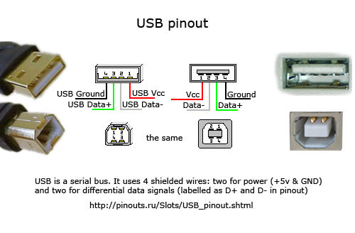
“Universal Serial Bus (USB) is an industry-standard that establishes specifications for cables and connectors and protocols for connection, communication, and power supply (interfacing) between computers, peripherals, and other computers. There have been four generations of USB specifications: USB 1.x, USB 2.0, USB 3.x, and USB4. USB device communication is based on pipes (logical channels). A pipe is a connection from the host controller to a logical entity within a device, called an endpoint. Because pipes correspond to endpoints, the terms are sometimes used interchangeably. Each USB device can have up to 32 endpoints (16 in and 16 out), though it is rare to have so many. Endpoints are defined and numbered by the device during initialization (the period after physical connection called “enumeration”) and so are relatively permanent, whereas pipes may be opened and closed. There are two types of pipe: stream and message. A message pipe is bi-directional and is used for control transfers. Message pipes are typically used for short, simple commands to the device, and for status responses from the device, used, for example, by the bus control pipe number 0. A stream pipe is a uni-directional pipe connected to a uni-directional endpoint that transfers data using an isochronous, interrupt, or bulk transfer” [Wikipedia].

“USB supplies power at 5 V ± 5% to power USB downstream devices. USB signals are transmitted using differential signaling on a twisted-pair data cable with 90 Ω ± 15% characteristic impedance. During USB communication, data is transmitted as packets. Initially, all packets are sent from the host via the root hub, and possibly more hubs, to devices. Some of those packets direct a device to send some packets in reply. The basic transactions of USB are OUT transaction, IN transaction, SETUP transaction, and Control transfer exchange” [Wikipedia].
Suggested Reading


The Ethernet standard came from the IEEE 802.3 Carrier Sense Multiple Access with Collision Detection (CSMA/CD) Access Method and Physical Layer Specifications, inspired by ALOHAnet from the University of Hawai’i. “The original 10BASE5 Ethernet uses coaxial cable as a shared medium, while the newer Ethernet variants use twisted pair and fiber optic links in conjunction with switches. Over the course of its history, Ethernet data transfer rates have been increased from the original 2.94 megabits per second (Mbit/s) to the latest 400 gigabits per second (Gbit/s). The Ethernet standards comprise several wiring and signaling variants of the OSI physical layer in use with Ethernet. Systems communicating over Ethernet divide a stream of data into shorter pieces called frames. Each frame contains the source and destination addresses, and error-checking data so that damaged frames can be detected and discarded; most often, higher-layer protocols trigger the retransmission of lost frames. As per the OSI model, Ethernet provides services up to and including the data link layer. The 48-bit MAC address was adopted by other IEEE 802 networking standards, including IEEE 802.11 Wi-Fi, as well as by FDDI, and EtherType values are also used in Subnetwork Access Protocol (SNAP) headers. Ethernet is widely used in homes and industries and works well with Wi-Fi. The Internet Protocol is commonly carried over Ethernet and so it is considered one of the key technologies that make up the Internet” [Wikipedia].

“In IEEE 802.3, a datagram is called a packet or frame. The packet is used to describe the overall transmission unit and includes the preamble, start frame delimiter (SFD), and carrier extension (if present). The frame begins after the start frame delimiter with a frame header featuring source and destination MAC addresses and the EtherType field giving either the protocol type for the payload protocol or the length of the payload. The middle section of the frame consists of payload data including any headers for other protocols (for example, Internet Protocol) carried in the frame. The frame ends with a 32-bit cyclic redundancy check, which is used to detect corruption of data in transit” [Wikipedia].
Suggested Reading

“SpaceWire is a spacecraft communication network based in part on the IEEE 1355 standard of communications. It is coordinated by the European Space Agency (ESA) in collaboration with international space agencies including NASA, JAXA, and RKA. Within a SpaceWire network, the nodes are connected through low-cost, low-latency, full-duplex, point-to-point serial links, and packet switching wormhole routing routers. SpaceWire covers two (physical and data-link) of the seven layers of the OSI model for communications. SpaceWire’s modulation and data formats generally follow the data strobe encoding – differential ended signaling (DS-DE) part of the IEEE Std 1355-1995. SpaceWire utilizes asynchronous communication and allows speeds between 2 Mbit/s and 400 Mbit/s, with an initial signaling rate of 10Mbit/s. DS-DE is well-favored because it describes modulation, bit formats, routing, flow control, and error detection in hardware, with little need for software. SpaceWire also has very low error rates, deterministic system behavior, and relatively simple digital electronics. SpaceWire replaced old PECL differential drivers in the physical layer of IEEE 1355 DS-DE with low-voltage differential signaling (LVDS). SpaceWire also proposes the use of space-qualified 9-pin connectors. SpaceWire and IEEE 1355 DS-DE allows for a wider set of speeds for data transmission and some new features for automatic failover. The fail-over features let data find alternate routes, so a spacecraft can have multiple data buses, and be made fault-tolerant. SpaceWire also allows the propagation of time interrupts over SpaceWire links, eliminating the need for separate time discrete.

SpaceWire is used all around the globe. Its use began primarily in ESA projects, but it is currently used by NASA, JAXA, RKA, and many other organizations and companies. Some NASA projects using it include the James Webb Space Telescope, Swift’s Burst Alert Telescope, the Lunar Reconnaissance Orbiter, LCROSS, the Geostationary Operational Environmental Satellite (GOES-R), and the SCaN Testbed, previously known as the Communications, Navigation, and Networking Reconfigurable Testbed (CoNNeCT). It has also been selected by the United States Department of Defense for Operationally Responsive Space. SpaceWire initiatives are being coordinated between several Space Agencies in the frame of CCSDS in order to extend its communication model to the Network and Transport Layers of the OSI model. SpaceWire supports highly fault-tolerant networks and systems, which is one reason for its popularity” [Wikipedia].

Suggested Reading

Serial ATA (SATA, abbreviated from Serial AT Attachment) is a computer bus interface that connects host bus adapters to mass storage devices and has become the predominant interface for storage devices, such as hard disk drives, optical drives, and solid-state drives. SATA data transfer rates range from 1.5 Gbit/s to 6 Gbit/s. Since these connectors are rarely seen outside the context of mass storage devices, we won’t delve further into SATA descriptions.

Integrated Computers

Now that we are familiar with all the parts that go into an onboard computer, we can talk about how these discrete components are integrated onto single or multiple boards. An onboard computer is an embedded computer, a computer that is integrated into a product, the spacecraft. Embedded computers do not usually have a keyboard, mouse, or monitor interface.
The detailed functional block diagram above is an example of an onboard computer that has many of the components we have surveyed. The crystal oscillator in the top left acts as the clock and there is a watchdog timer to detect faults lower in that first column. To the right of the clock, the CPU is downstream of the clock and watchdog signals and upstream of commands sent to the system bus. The CPU also interacts with a direct memory access (DMA) controller, a type of RAM, and a local bus, which funnels data from the data bus. To the far right, we have ROM and RAM, receiving data through the data bus from the system bus. Everything above the system bus dividing line consists of the guts of an onboard computer. Everything below the system bus dividing line interfaces to peripheral systems, like power, telecommunications, payloads, etc. Working from the left to the right and from the bottom towards the system bus, the J12 connector communicates bidirectional signals from a subsystem to CMOS drivers through a UART interface through a data bus to finally reach the system bus. The J12 connector also interfaces with a telecommunication interface through the radio frequency (RF) interface through a data bus to finally reach the system bus. You can work down the line of how the other subsystem components communicate to the system bus; the take-home message is that the interfaces are specific to the subsystem it must accommodate and must funnel the signals into the system bus in a uniform manner.

.svg)